
SLVS-EC Receiver IP
Compliant with Version 2.0 / Compliant with Version 3.1
What is SLVS-EC?
SLVS-EC (Scalable Low Voltage Signaling with Embedded Clock) is a high-speed, high-performance serial interface implemented in Sony’s CMOS image sensors.
Unlike conventional LVDS, the clock is embedded within the data, allowing PCB design without having to worry about skew between serial buses.
A new interface that delivers “faster, lower power, and simpler” performance. That is SLVS-EC.
Lineup
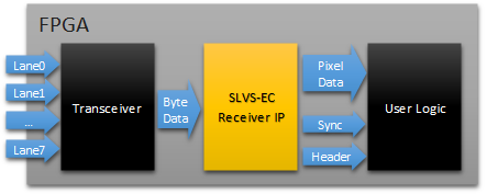
SLVS-EC RX IP

SLVS-EC RX is a receiver IP that supports SLVS-EC ver 2.0.
It analyzes SLVS-EC data received via the FPGA's high-speed transceivers and extracts and outputs header information and pixel data.It is also designed with a focus on minimizing FPGA resource consumption while supporting payload error detection and error correction (optional).
By combining this IP with your logic, you can optimize the resource usage of the entire system.
SLVS-EC3 RX IP

SLVS-EC3 RX is a receiver IP that supports SLVS-EC ver 3.1.
In addition to the features supported by the conventional SLVS-EC RX IP, it also supports GCC (Gigabit Channel Coding), which was introduced in SLVS-EC ver 3.0 and later.GCC is a coding scheme that improves transmission efficiency compared to conventional 8b/10b encoding.
Using this IP enables high-speed data transmission of up to 12.5 Gbps per lane, as specified in SLVS-EC ver 3.1.
Support
CIS employs numerous engineers with extensive experience in various fields, including RTL design related to high-speed interfaces and image processing, PCB design involving high-speed signals, and embedded software development. Please feel free to contact us regarding IP customization and other related matters.