SLVS-EC Receiver IP
SLVS-EC Receiver IP
What is SLVS-EC?
SLVS-EC(Scalable Low Voltage Signaling with Embedded Clock)is a high speed, high performance interface for 4th generation Sony CMOS image sensors. SLVS-EC differs from conventional LVDS interface in that the clock is embedded in the data, allowing circuit design without considering the pesky skew between serial buses.
In a nut shell, SLVS-EC enables faster, lower power design made easy.
SLVS-EC Receiver IP Overview
CIS has concentrated on extracting pixel data from the byte data received via FPGA’s high speed transceiver, enabling an IP with low resource usage. We provide reference design along with this IP.
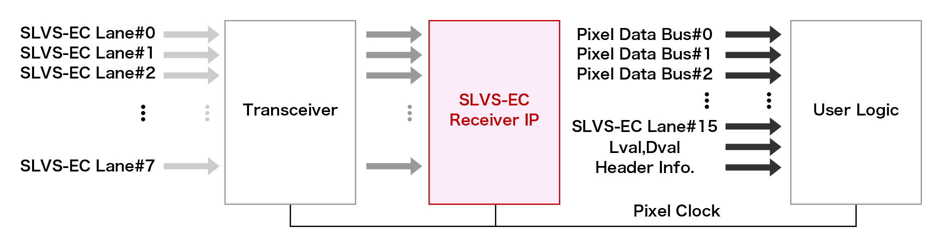
SLVS-EC Receiver IP Details
Specifications
| Version | SLVS-EC v2.0 compliant |
|---|---|
| Number of input lanes | 1,2,4,6,8 |
| Number of output buses | 2,4,8,12,16 (2x the number of input lanes) |
| RAW format | RAW8,10,12,14,16 |
| Line length | 4 ~ ∞ |
| ECC option | N.A. |
| CRC option | N.A. |
| Baud rate | Grade1~Grade3 (Possible by transceiver setting) |
| Header information output | Frame Start/End, Line Valid, Line Number, EBD Line, Data ID, Header CRC Error |
Resource Usage
Resource usage on AMD AC701 board as follows:
| Resource | Company A | CIS |
| Register | 9654 | 1724 |
|---|---|---|
| LUT | 6179 | 3827 |
| Block RAM | 4 | 0 |
Supported Devices
Supports AMD 7 series FPGAs. For Intel FPGAs, please consult us.
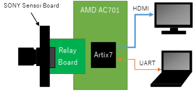
Demonstration Environment
Demonstration of up to 2 lanes possible by use of AMD AC701 Sony image sensor board. Support for KC705 board (max. 4 lanes), VC707 (max. 8 lanes) possible by way of preparing a relay board.
Support
We have a dedicated FPGA and software design team comprising 15 seasoned engineers specializing in high speed interface, image processing and embedded software design and development. Please feel free to contact us on whatever project you have in mind.